

 الفيزياء الكلاسيكية
 الكهربائية والمغناطيسية
 علم البصريات
 الفيزياء الحديثة
 النظرية النسبية
 الفيزياء النووية
 فيزياء الحالة الصلبة
 الليزر
 علم الفلك
 المجموعة الشمسية
 الطاقة البديلة
 الفيزياء والعلوم الأخرى
 مواضيع عامة في الفيزياء
|
Read More
Date: 8-5-2017
Date: 14-5-2017
Date: 8-5-2017
|
Velocity Saturation
So far in our discussion of drift velocity, we have assumed that mobility is not a function of electric field, meaning that the drift velocity will increase linearly with applied electric field. The total velocity of a particle is the sum of the random thermal velocity and drift velocity. At T = 300 K, the average random thermal energy is given by
 (1)
(1)

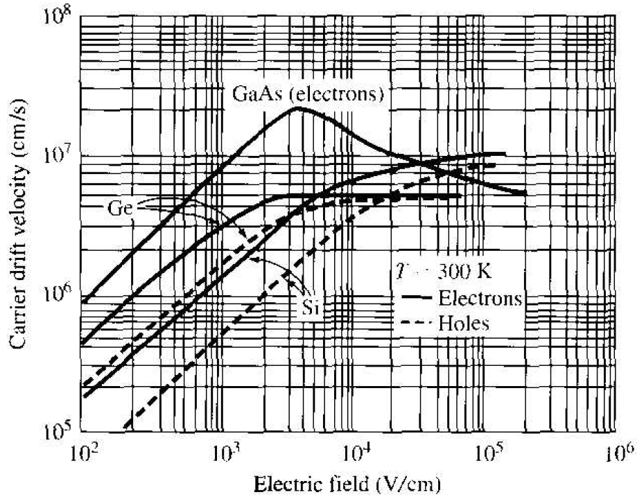
Figure 1.1 Carrier drift velocity versus electric field for high-purity silicon. germanium, and gallium arsenide.
This energy translates into a mean thermal velocity of approximately 107 cm/s for an electron in silicon. If we assume an electron mobility of μn = 1350 cm2/V-s in low doped silicon, a drift velocity of 105 cm/s, or 1 percent of the thermal velocity, is achieved if the applied electric field is approximately 75 V/cm. This applied electric field does not appreciably alter the energy of the electron.
Figure 1.1 is a plot of average drift velocity as a function of applied electric field for electrons and holes in silicon, gallium arsenide, and germanium. At low electric fields, where there is a linear variation of velocity with electric field, the slope of the drift velocity versus electric field curve is the mobility. The behavior of the drift velocity of carriers at high electric fields deviates substantially from the linear relationship observed at low fields. The drift velocity of electrons in silicon, for example. saturates at approximately 107 cm/s at an electric field of approximately 30 kV/cm. If the drift velocity of a charge carrier saturates, then the drift current density also saturates and becomes independent of the applied electric field.
The drift velocity versus electric field characteristic of gallium arsenide is more complicated than for silicon or germanium. At low fields, the slope of the drift velocity versus E-field is constant and is the low-field electron mobility, which is approximately 8500 cm2/V-s for gallium arsenide. The low-field electron mobility in gallium arsenide is much larger than in silicon. As the field increases, the electron drift velocity in gallium arsenide reaches a peak and then decreases. A differential mobility is the slope of the vd , versus E curve at a particular point on the curve and the negative slope of the drift velocity versus electric field represents a negative differential mobility. The negative differential mobility produces a negative differential resistance; this characteristic is used in the design of oscillators.

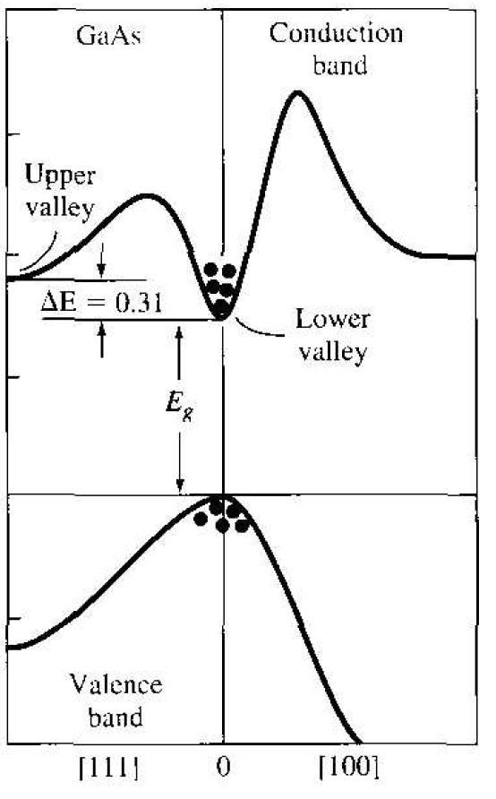
Figure 1.2 Energy-hand structure for gallium arsenide showing the upper valley and lower valley in the conduction band.
The negative differential mobility can be understood by considering the E versus k diagram for gallium arsenide, which is shown again in Figure 1.2. The density of states effective mass of the electron in the lower valley is m*n = 0.067m0. The small effective mass leads to a large mobility. As the E-field increases. the energy of the electron increases and the electron can be scattered into the upper valley, where the density of states effective mass is 0.55m0. The larger effective mass in the upper valley yields a smaller mobility. This intervalley transfer mechanism results in a decreasing average drift velocity of electrons with electric field, or the negative differential mobility characteristic.


|
|
|
|
التوتر والسرطان.. علماء يحذرون من "صلة خطيرة"
|
|
|
|
|
|
|
مرآة السيارة: مدى دقة عكسها للصورة الصحيحة
|
|
|
|
|
|
|
نحو شراكة وطنية متكاملة.. الأمين العام للعتبة الحسينية يبحث مع وكيل وزارة الخارجية آفاق التعاون المؤسسي
|
|
|