
تاريخ الرياضيات

الاعداد و نظريتها

تاريخ التحليل

تار يخ الجبر

الهندسة و التبلوجي


الرياضيات في الحضارات المختلفة

العربية

اليونانية

البابلية

الصينية

المايا

المصرية

الهندية


الرياضيات المتقطعة

المنطق

اسس الرياضيات

فلسفة الرياضيات

مواضيع عامة في المنطق


الجبر

الجبر الخطي

الجبر المجرد

الجبر البولياني

مواضيع عامة في الجبر

الضبابية

نظرية المجموعات

نظرية الزمر

نظرية الحلقات والحقول

نظرية الاعداد

نظرية الفئات

حساب المتجهات

المتتاليات-المتسلسلات

المصفوفات و نظريتها

المثلثات


الهندسة

الهندسة المستوية

الهندسة غير المستوية

مواضيع عامة في الهندسة

التفاضل و التكامل


المعادلات التفاضلية و التكاملية

معادلات تفاضلية

معادلات تكاملية

مواضيع عامة في المعادلات


التحليل

التحليل العددي

التحليل العقدي

التحليل الدالي

مواضيع عامة في التحليل

التحليل الحقيقي

التبلوجيا

نظرية الالعاب

الاحتمالات و الاحصاء

نظرية التحكم

بحوث العمليات

نظرية الكم

الشفرات

الرياضيات التطبيقية

نظريات ومبرهنات


علماء الرياضيات

500AD

500-1499

1000to1499

1500to1599

1600to1649

1650to1699

1700to1749

1750to1779

1780to1799

1800to1819

1820to1829

1830to1839

1840to1849

1850to1859

1860to1864

1865to1869

1870to1874

1875to1879

1880to1884

1885to1889

1890to1894

1895to1899

1900to1904

1905to1909

1910to1914

1915to1919

1920to1924

1925to1929

1930to1939

1940to the present

علماء الرياضيات

الرياضيات في العلوم الاخرى

بحوث و اطاريح جامعية

هل تعلم

طرائق التدريس

الرياضيات العامة

نظرية البيان
CIRCUITS FOR ARITHMETIC COMPUTATION-Logical circuit elements
المؤلف:
J. ELDON WHITESITT
المصدر:
BOOLEAN ALGEBRA AND ITS APPLICATIONS
الجزء والصفحة:
138-142
28-12-2016
1920
We have already introduced two devices which can be connected into circuits for useful purposes, namely, relays and manual switches. In the construction of electronic computers, other devices are more frequently used. Circuit elements involving diodes or vacuum tubes are very common. Rather than discuss the many types of electronic apparatus that may be used, we will introduce the idea of a logical circuit element. It will be enough to know that these elements can be constructed; in fact, commercially packaged elements of these types, suitable for use in many types of equipment, can be purchased directly.
Whether these elements are constructed from relays or tubes, or other basic parts, will be immaterial in most of this chapter. The student may think in terms of relays, since, as we will show, it is possible to construct all the logical elements from relays alone. Often these relay circuits have very poor operating characteristics in comparison with circuits involving other components, but we will leave the discussion of electronic components to more advanced texts on computer design.
We will conceive of a logical circuit element as a little box or package with one or more input leads (wire connections) and one or more output leads. These leads will carry signals in the form of positive voltage corresponding to a value 1, or zero voltage corresponding to a value 0. We will use a single letter, say x, to stand for the condition of the lead. When the lead carries a signal, we will say that x takes on the value 1. When the lead does not carry a signal, we say that x has the value 0. This represents only a slight modification of our earlier point of view, where 1 and 0 meant closed or open circuits, since we can think of a closed circuit as one carrying a signal, and of an open circuit as one incapable of carrying a signal. Other signals than that of a positive voltage could be used equally well, and in fact the signal used will in general depend on the type of components used in circuit construction. We will use just this one type of signal for simplicity, and we will adapt all our circuits to its use.
We will diagram a circuit element as a circle with a letter inside to designate the type of element, and with lines indicating inputs and outputs. Arrows on these lines will indicate the difference between input and output, an arrow pointing toward the circle being used on each input.
The first logical circuit element we will consider has a single input and a single output. The function of this element is to obtain the complement of a given signal; that is, the output is 0 when the input is 1, and conversely.
Figure 1-1 shows the notation we will use, a circle with C in the center, and one possible construction for this element in terms of relays. The input is designated x, so the output is x'.

FIG. 1-1. (a) Symbolic notation and (b) circuit for a complement.
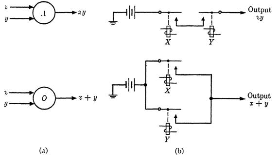
The next two logical circuit elements correspond to the logical connections "and" and "or." Each may have two or more inputs and only a single output. The "and" element is shown in diagrams as a circle with A in the center. This element produces an output signal (output has value 1) if and only if every input carries a signal (has value 1). If the inputs to an "and" element are x, y, and z, for example, the output function may be written as xyz, where the notation is that of Boolean algebra. The "or" element, represented graphically by a circle with 0 in the center, produces an output signal whenever one or more inputs carry a signal. If the inputs to an "or" element are x, y, and z, for example, the output is the Boolean function x + y + z. Figure 1-2 shows the symbolic notations for these elements and possible circuits to realize the elements. Each is shown with only two inputs; the extension to more inputs is self-evident. Many other circuits, with these or other components, are possible.
A final logical circuit element will be termed a flip-flop and designated by a circle with an F in the center. This device has a single input and a

FIG. 1-2. "And" and "or" logical circuit elements.

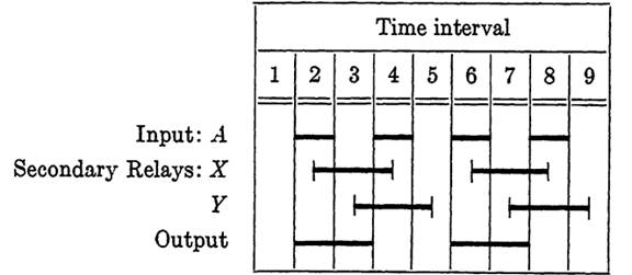
FIG. 1-3. Sequence chart for a flip-flop.

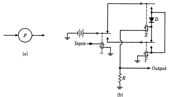
FIG. 1-4. (a) Symbolic notation and (b) circuit for a flip-flop.
single output. It has two stable states, in one of which the output is 1, in the other of which the output is 0. The state of the flip-flop changes each time a signal appears (even momentarily) on the input lead, whereupon it maintains the new state and corresponding output until the next signal is received.
We will design a flip-flop by the methods of (RELAY CIRCUITS AND CONTROL PROBLEMS). The sequence chart of Fig. 1-3 represents the desired output in terms of input signals that occur intermittently. A choice of operating sequence for two secondary relays, sufficient to give the desired output, is also shown. The control functions for X and Y are: Fx= ay' + a'x and Fy= a'x - ay. The output function is ay' + a'x, which is identical to F. Because these two functions are the same, the simplest way to get the desired output is directly from the control path of X, as shown in Fig. 1-4(b). A make contact on X could also be used (although this would cause a slight delay), giving an output sequence identical with the operate sequence of X. Either method would serve our purpose.
The flip-flop symbol to be used in future diagrams and the actual relay circuit that it represents are shown in Fig. 1-4. The symbol at D indicates a rectifying diode to prevent the sneak path which would otherwise cause Y to operate when A is operated and Y released. This flip-flop could be constructed more simply by using vacuum tubes.
 الاكثر قراءة في الجبر البولياني
 اخر الاخبار
اخبار العتبة العباسية المقدسة

الآخبار الصحية


 قسم الشؤون الفكرية يصدر كتاباً يوثق تاريخ السدانة في العتبة العباسية المقدسة
 "المهمة".. إصدار قصصي يوثّق القصص الفائزة في مسابقة فتوى الدفاع المقدسة للقصة القصيرة
 (نوافذ).. إصدار أدبي يوثق القصص الفائزة في مسابقة الإمام العسكري (عليه السلام)


